eic-projdet-pfrich-electronics-l AT lists.bnl.gov
Subject: ePIC pfRICH electronics mailing list
List archive
Re: [Eic-projdet-pfrich-electronics-l] Address pin
- From: Pierrick Dinaucourt <pdinaucourt AT omega.in2p3.fr>
- To: "Kiselev, Alexander" <ayk AT bnl.gov>, Miklos Czeller <miklos.czeller AT cern.ch>
- Cc: Gabor Nagy <hunagabo AT gmail.com>, "Cacace, Daniel" <dcacace AT bnl.gov>, Damien Thienpont <damien.thienpont AT in2p3.fr>, "Camarda, Timothy via Eic-projdet-pfrich-electronics-l" <eic-projdet-pfrich-electronics-l AT lists.bnl.gov>
- Subject: Re: [Eic-projdet-pfrich-electronics-l] Address pin
- Date: Thu, 9 Nov 2023 08:51:35 +0100
Hi Alexander,
it's ok for me to change the adress it's quick and will do it
today.
Regards
Pierrick
Le 08/11/2023 à 17:31, Kiselev,
Alexander a écrit :
Hello colleagues,
we keep forgetting a fraction of people on Cc in some of our e-mail threads. At a risk of flooding the innocent people's mailboxes, let's use the mailing list for such discussions (see it on the Cc), which is also good for the archiving purposes.
Concerning the ASIC numbering scheme, I'd definitely prefer to use 0..7 for both halves if Pierrick is willing to make this change. In case we stick to 0..15, I have no preference between using a hardwired GND / NC pins or assigning even and odd IP addresses to the respective halves via a dipswitch.
Cheers, Alexander.
From: Miklos
Czeller <miklos.czeller AT cern.ch>
Sent: Wednesday, November 8, 2023 11:13 AM
To: Kiselev, Alexander <ayk AT bnl.gov>
Cc: Gabor Nagy <hunagabo AT gmail.com>; pdinaucourt AT omega.in2p3.fr <pdinaucourt AT omega.in2p3.fr>; Cacace, Daniel <dcacace AT bnl.gov>; Damien Thienpont <damien.thienpont AT in2p3.fr>
Subject: Re: Address pin
Sent: Wednesday, November 8, 2023 11:13 AM
To: Kiselev, Alexander <ayk AT bnl.gov>
Cc: Gabor Nagy <hunagabo AT gmail.com>; pdinaucourt AT omega.in2p3.fr <pdinaucourt AT omega.in2p3.fr>; Cacace, Daniel <dcacace AT bnl.gov>; Damien Thienpont <damien.thienpont AT in2p3.fr>
Subject: Re: Address pin
Hi Alex,
You wrote earlier:
"Please,
as we discussed yesterday: number the ASICs from 0 to 7 in
each of the two halves (top eight and bottom eight on all
our pictures). Pierrick, at some point we need a picture,
which shows the ASIC IDs."
So, I think both halves use address from 0-7. Pierrick,
can you confirm it?
Otherwise,
I think this is the best solution. Because in this case the
FPGA FW should be the same for both halves.
I
asked for the identification pin so that I could easily
decide which side the signal was coming from. Here it is
possibility to show the address range 0-15 to the computer,
or we can use this ID pin as a flag which is identifies the
half in the communication packages. This is our decision...
I
asked for the two previous things (DIP switch and ID Pin) to
prepare for everything what I see now.
Don't
worry about the many versions. Everyone will receive a
unique FW. In the compiled version there will be no
unnecessary stuff. Only in the repository, but that doesn't
matter.
I
just don't want to have to implement the same or very
similar functions in multiple ways.
Cheers,
M!klos
ps.:
I pressed the wrong button earlier (Reply vs. Reply All).
I've now put everybody back in the mail stream. Sorry!
From: Kiselev,
Alexander <ayk AT bnl.gov>
Sent: Wednesday, November 8, 2023 2:36 PM
To: Miklos Czeller <miklos.czeller AT cern.ch>
Subject: Re: Address pin
Hi Miklos,
Sent: Wednesday, November 8, 2023 2:36 PM
To: Miklos Czeller <miklos.czeller AT cern.ch>
Subject: Re: Address pin
we need to spell several things out explicitly before anything goes into manufacturing. Right now I'm sure Pierrick uses 0..15 ASIC IDs on his board.
I understand the desire to keep the same firmware for all tasks which you have to manage. If I may suggest, in this case there should be an option to turn certain features off completely. A good example is turning off the ASIC trigger lines information handling entirely rather than depending on the threshold setting inside of the ASIC, which at the end can always generate a spurious L1A command. Can we agree on this?
Cheers, Alexander.
From: Miklos
Czeller <miklos.czeller AT cern.ch>
Sent: Wednesday, November 8, 2023 1:58 AM
To: Kiselev, Alexander <ayk AT bnl.gov>
Subject: Re: Address pin
Hi Alex,
Sent: Wednesday, November 8, 2023 1:58 AM
To: Kiselev, Alexander <ayk AT bnl.gov>
Subject: Re: Address pin
I
haven't thought through exactly how the packages will be. I
will get there soon. But we'll talk about that later.
What
I definitely want is that the ASIC addresses are between 0
and 7 (on both sides). It is not changed.
I
want to maintain the options for different solutions if they
are not expensive. That's why I asked for the DIP switch and
that one connection to the connector.
(
Since I want to use the ethernet with the KCU as well, I
need the dip switch. Currently I am using the onboard switch
for other things. )
The
FW so far it looks like we'll be using it in 8 different
places or ways. There are some features you don't need, but
I don't want to take them out of the FW until I have to, so
I don't have to deal with a lot of branches.
Cheers,
M!klos
From: Kiselev,
Alexander <ayk AT bnl.gov>
Sent: Tuesday, November 7, 2023 10:47 PM
To: Miklos Czeller <miklos.czeller AT cern.ch>
Subject: Re: Address pin
Hi Miklos,
Sent: Tuesday, November 7, 2023 10:47 PM
To: Miklos Czeller <miklos.czeller AT cern.ch>
Subject: Re: Address pin
now I'm confused. I thought I will be addressing a particular ASIC via {IP, 0..7} pair of numbers, and then the FPGA sitting on this IP will decide whether to address its eight ASICs as 0..7 or 8..15 depending on whether a particular pin is GND or NC. No?
Concerning the dipswitch, I understand you want to set the lower four bits of the IP address, to be added to a common base. I was just puzzled, that you (1) did not specify any circuitry involved, (2) requested this feature on a passive board without ethernet connector.
By the way, my other equipment (DREAM electronics by Saclay) is using subnet 192.168.10.* with hardcoded IPs. It may make sense to use the same gigabit switch for HGCROCs. Addresses .2, .32, .112 and .131 are occupied, just in case, but one can obviously find a continuous range of ten addresses. The switch supports jumbo frames.
Cheers, Alexander.
From: Miklos
Czeller <miklos.czeller AT cern.ch>
Sent: Tuesday, November 7, 2023 3:26 PM
To: Kiselev, Alexander <ayk AT bnl.gov>
Subject: Fw: Address pin
Hello Alex,
Sent: Tuesday, November 7, 2023 3:26 PM
To: Kiselev, Alexander <ayk AT bnl.gov>
Subject: Fw: Address pin
(1)
Miklos:
do I get it right that this modification means the IDs will
effectively be 0..7 from the DAQ perspective? I mean you
convert these IDs to 0..15 internally, on your end?
Yes
You are right.
From
the computer you will see address 0..15. But actually the
address goes up to 0..7.
(2) Miklos: not sure I understand the idea? this switch is supposed to be connected where? This can be useful when boards need to be distinguished. I don't want to implement DHCP protocol from vhdl in the first place. So, for setting fixed addresses it might come in handy. This will connected to the FPGA
(3) Somebody will give me information on what and how I will see on the trigger line. Not necessarily now, but in the near future...
Cheers, M!klos
From: Miklos
Czeller <Miklos.Czeller AT mediso.com>
Sent: Tuesday, November 7, 2023 6:44 PM
To: Miklos Czeller <miklos.czeller AT cern.ch>
Subject: Fwd: Address pin
Sent: Tuesday, November 7, 2023 6:44 PM
To: Miklos Czeller <miklos.czeller AT cern.ch>
Subject: Fwd: Address pin
Sent From My iPhone
Továbbított levél kezdete:
Feladó: "Kiselev, Alexander" <ayk AT bnl.gov>
Dátum: 2023. november 7. 17:29:23 CET
Címzett: nagy g <hunagabo AT gmail.com>, Pierrick Dinaucourt <pdinaucourt AT omega.in2p3.fr>
Másolat: "Damien Thienpont (IN2P3)" <damien.thienpont AT in2p3.fr>, "Cacace, Daniel" <dcacace AT bnl.gov>, Miklos Czeller <Miklos.Czeller AT mediso.com>
Tárgy: Válasz: Address pin
Hello colleagues,
few clarifying questions to (1)..(3):
(1) Miklos: do I get it right that this modification means the IDs will effectively be 0..7 from the DAQ perspective? I mean you convert these IDs to 0..15 internally, on your end?
(2) Miklos: not sure I understand the idea? this switch is supposed to be connected where?
(3) Pierrick: are you really going to pass this timing signal to a "free" channel (one of the 64..71) on every ASIC (or one ASIC of each pair)? this would be great. please confirm
(3) Gabor, Pierrick: did we ever agree on the TRIG_Gx signal standard?
Cheers, Alexander.
From: nagy g <hunagabo AT gmail.com>
Sent: Tuesday, November 7, 2023 9:13 AM
To: Pierrick Dinaucourt <pdinaucourt AT omega.in2p3.fr>; Kiselev, Alexander <ayk AT bnl.gov>
Cc: Damien Thienpont (IN2P3) <damien.thienpont AT in2p3.fr>; Cacace, Daniel <dcacace AT bnl.gov>; Miklos Czeller <miklos.czeller AT mediso.com>
Subject: Address pinHi Pierrick and Alexander,
1. Miklos asked me to add a pin to the FMC/passive board if that is still possible, which could identify, what half of the ASIC board is connected to the FPGA (via the passive board). Basically it would mean that, one of the pin on the ERM5 connector (like the pin38?) need to be connected to GND on one half (like the connector of ASICs M7,M8) and would be floating on the other half of the ASICs (like the connectors of M15 and M16).
Could you confirm if that is still possible?
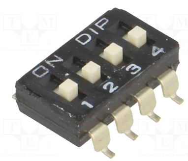
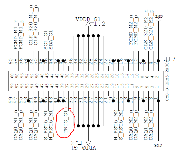
2. Another request from Miklos is that, for testing the Ethernet connection with the KCU105 board via the FMC/passive board) would be useful to add a address switch to the FMC/passive board. Like a 4 bit dipswitch. Something like this:3. and the final thing is the TRIG_G1 signal on the ASICs board. Could you confirm that, this trigger line is only connected to one ASIC, and the others like TRIG_G2/3/4 is not connected?
Thanks, gabor
This e-mail may contain confidential and/or copyrighted information and is intended solely for the person or organization to whom it is addressed. If you receive this e-mail in a damaged form, or erroneously or if you are not the intended recipient, please inform the sender immediately and delete this e-mail from your system. Unauthorised copying, distribution, modification, or disclosure of this e-mail is strictly forbidden.
E-mails are primarily sent for information purposes. The Mediso Medical Imaging Systems Ltd. neither undertakes nor acknowledges any official obligations via e-mails, unless the parties have agreed otherwise.
--
Pierrick Dinaucourt
PCB Designer
Laboratoire OMEGA
Unité CNRS-Polytechnique
tél: 01-69-33-89-83
-
Re: [Eic-projdet-pfrich-electronics-l] Address pin,
Kiselev, Alexander, 11/08/2023
-
Re: [Eic-projdet-pfrich-electronics-l] Address pin,
Pierrick Dinaucourt, 11/09/2023
- Re: [Eic-projdet-pfrich-electronics-l] Address pin, Kiselev, Alexander, 11/09/2023
-
Re: [Eic-projdet-pfrich-electronics-l] Address pin,
Pierrick Dinaucourt, 11/09/2023
Archive powered by MHonArc 2.6.24.

