eic-projdet-pfrich-electronics-l AT lists.bnl.gov
Subject: ePIC pfRICH electronics mailing list
List archive
[Eic-projdet-pfrich-electronics-l] Fw: pfRICH prototype HGCROC3 ASIC & FPGA cooling scheme
- From: "Kiselev, Alexander" <ayk AT bnl.gov>
- To: "Camarda, Timothy via Eic-projdet-pfrich-electronics-l" <eic-projdet-pfrich-electronics-l AT lists.bnl.gov>
- Subject: [Eic-projdet-pfrich-electronics-l] Fw: pfRICH prototype HGCROC3 ASIC & FPGA cooling scheme
- Date: Thu, 10 Aug 2023 12:56:19 +0000
Forwarding this whole thread to the list.
From: Kiselev, Alexander <ayk AT bnl.gov>
Sent: Thursday, August 10, 2023 8:51 AM
To: nagy g <hunagabo AT gmail.com>
Cc: Czeller Miklos <czeller.miklos AT gmail.com>; Damien Thienpont (IN2P3) <damien.thienpont AT in2p3.fr>; Pierrick Dinaucourt <pdinaucourt AT omega.in2p3.fr>; Cacace, Daniel <dcacace AT bnl.gov>; Norbert Novitzky <Norbert.Novitzky AT cern.ch>; Alexey Lyashenko <alyashenko AT incomusa.com>
Subject: Re: pfRICH prototype HGCROC3 ASIC & FPGA cooling scheme
Hi Gabor,
Looks good to me. Alexey, can you confirm please that we can use the proposed standoffs rather than nuts for four screws, as shown in the drawing? I'm actually not sure this is a good idea, since the force when mating the ERF/Ms will be eventually translated
to the sensor itself. I'd rather increase the Samtec connector profile height if needed, and use back side pressfit fixtures the way you show this in the present model. Concerning power distribution, if 1A is too much for Samtec connector pins, we should probably
foresee a separate LV F/M pair of connectors, or perhaps just add a short cable connecting the two boards in this first iteration.
Have a nice vacation!
Cheers,
Alexander.
From: nagy g <hunagabo AT gmail.com>
Sent: Thursday, August 10, 2023 3:26 AM
To: Kiselev, Alexander <ayk AT bnl.gov>
Cc: Czeller Miklos <czeller.miklos AT gmail.com>; Damien Thienpont (IN2P3) <damien.thienpont AT in2p3.fr>; Pierrick Dinaucourt <pdinaucourt AT omega.in2p3.fr>; Cacace, Daniel <dcacace AT bnl.gov>; Norbert Novitzky <Norbert.Novitzky AT cern.ch>
Subject: Re: pfRICH prototype HGCROC3 ASIC & FPGA cooling scheme
Hi Alexander,
Since my email, Pierric sent me a model where the ASICS are pushed away from the midle of the cells, and it looks like the option 2 FPGA (control) board can fit easily into that design even with the screws between the B2B (ERF5/ERM5)
connectors:
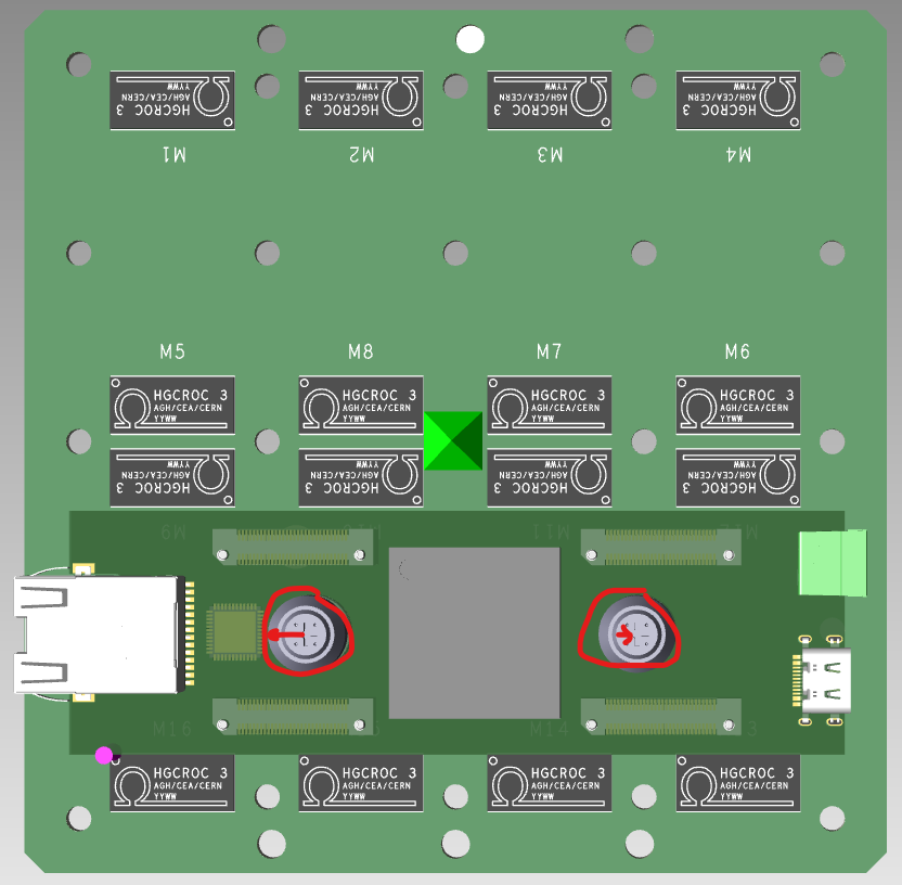
I need to modify a bit the screw positions to utilize the already existing holes, but that looks okay. Only the thread size and type is the question, but that does not seems to be an urgent decision.
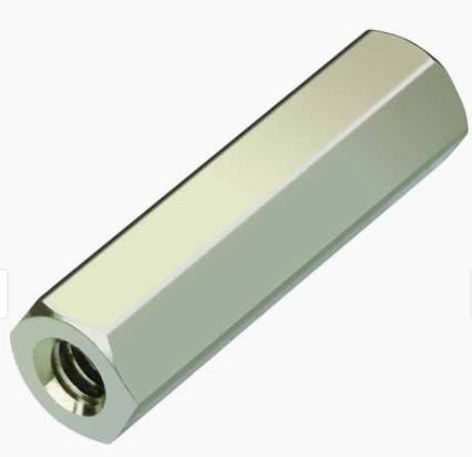
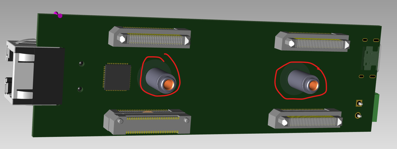
The usage of press-fit or solderable standoffs also looks vanished, as with this design we can utilize the already existing holes and screws between the detector's ceramic and the sensor board; we just need to make them a bit longer or add a threaded pillar/standoff
like this:
So in this case we can replace this ones:
There is a power-related question that popped up with the email from Pierrick. Namely, the ASICs need
1A AT 1.2V per each, which (was not clear for me until now) should be created on the FPGA board. It needs a bit of calculation to see how much power we will create on the control board all together...
But basically it is getting clear what we need to do :)
BTW, I will be out for two weeks from today with limited access to my mail, and as I learned yesterday, Pierric will also be on Holidays for the next three weeks.
Have a Great Day!
gabor
Kiselev, Alexander <ayk AT bnl.gov> ezt írta (időpont: 2023. aug. 10., Cs, 2:41):
Hi Gabor,
as a person who typically does not document anything (and even worse, forgets himself what was done half a year ago 🙂), I can only appreciate this effort. Few specific comments:
slide 1: I thought we wanted to place the ASICs further away towards the edge of the FPGA board footprint (and move Samtec connectors closer to each other, as you also indicate in the subsequent slides)
slide 2: it is unlikely, but can happen that -0.50- ERF(M)5 connectors do not provide enough clearance to accommodate the screws / nuts which attach ASIC PCB to the sensor. -0.70- may be a better choice, but let me ask Alexey Lyashenko from Incom give you the screws (nuts) specs, as we see them now
slide 2: what is a problem with Jumbo frames? We routinely use such a configuration for the gas detector readout (DREAM by Saclay, UDP), and I guess eventually in the test beam there will be a single gigabit switch shared by DREAM FEEs and your HGCROC implementation cards, with Jumbo frame support, and perhaps a 10G uplink to the host PC
slide 5: 100mm x 42mm sounds great to me, but it is not clear how LV is distributed. Do I get it right that ASICs receive power via Samtec connectors, and we end up with a pair of LV cables per sensor (one per FPGA board)?
slide 6: I recall ERF5 only has 5mm and 7mm height options. Are the other ones non-standard? IN this case we should certainly avoid them, because of the limited supply and long lead times
slide 6: I think we should be able to machine these heat sinks to a shape we need, but still have them as a single piece, to simplify integration. Daniel can correct me, but I think that by using gap pads we are not really too much sensitive to a possible few hundred um FPGA and ASIC top surface "height" mismatch, to provide a good thermal contact to both of them
Concerning pressfit & Co, my gut feeling is that we want to avoid top mount pressfit standoffs, because they are most likely not designed to withstand a force when mounting. Anything which is bottom mounted looks more reliable to me, but we may want to introduce counterbores in the ASIC PCB, since PCB-to-sensor clearance will be only 1.0mm
Cheers,Alexander.
From: nagy g <hunagabo AT gmail.com>
Sent: Tuesday, August 8, 2023 2:48 PM
To: Kiselev, Alexander <ayk AT bnl.gov>; Czeller Miklos <czeller.miklos AT gmail.com>; Damien Thienpont (IN2P3) <damien.thienpont AT in2p3.fr>; Pierrick Dinaucourt <pdinaucourt AT omega.in2p3.fr>; Cacace, Daniel <dcacace AT bnl.gov>
Cc: Norbert Novitzky <Norbert.Novitzky AT cern.ch>
Subject: Re: pfRICH prototype HGCROC3 ASIC & FPGA cooling schemeHi All,
I tried to follow the mailing threads, but to be honest, I have lost a few times (and I'm really sorry for that)... so I tried to put together a document about all the information I could gather so far.I could also spend some time creating/collecting mechanical models, so I made some board concept pictures based on Alexander, Miklos, Daniel, and Damien's previous models and comments.Please comment on that.
Best Regards,gabor
Kiselev, Alexander <ayk AT bnl.gov> ezt írta (időpont: 2023. aug. 4., P, 3:38):
Hi Daniel,
I think the easiest would be to go to https://www.samtec.com/products/erf5 ,
configure ERM5-030-05.0-L-DV-TR (or -07.0-) and choose the most convenient CAD format to download (there are literally dozens available). Same for a matching ERF5 connector.
Cheers,Alexander.
From: Cacace, Daniel <dcacace AT bnl.gov>
Sent: Thursday, August 3, 2023 8:18 PM
To: nagy g <hunagabo AT gmail.com>
Cc: Kiselev, Alexander <ayk AT bnl.gov>
Subject: Re: pfRICH prototype HGCROC3 ASIC & FPGA cooling schemeHi Gabor,
Sure, I can take a look at the mating connectors to the mechanical model. Could you point me to the corresponding part files?
From: nagy g <hunagabo AT gmail.com>
Sent: Thursday, August 3, 2023 12:36 PM
To: Kiselev, Alexander <ayk AT bnl.gov>
Cc: Cacace, Daniel <dcacace AT bnl.gov>; czeller.miklos AT gmail.com <czeller.miklos AT gmail.com>; Damien Thienpont (IN2P3) <damien.thienpont AT in2p3.fr>; Pierrick Dinaucourt <pdinaucourt AT omega.in2p3.fr>
Subject: Re: pfRICH prototype HGCROC3 ASIC & FPGA cooling schemeHi Alexander,
I agree and sure we can go further to work out the details, but I would appreciate, if Daniel (?) could add the mating connectors to the mechanical model (like Ethernet) just to see if they can be connected with the tiling setup as well. (even the connectors within the base PCB contour.)But basically I am happy with this configuration as it seems to be feasible.
The model what I sent is created by Miklos, so I will do my own one and will add the solderable standoffs or the pressfit bolts (based on what is available).
Br, gabor
Kiselev, Alexander <ayk AT bnl.gov> ezt írta (időpont: 2023. aug. 3., Cs, 13:54):
Hi Gabor,
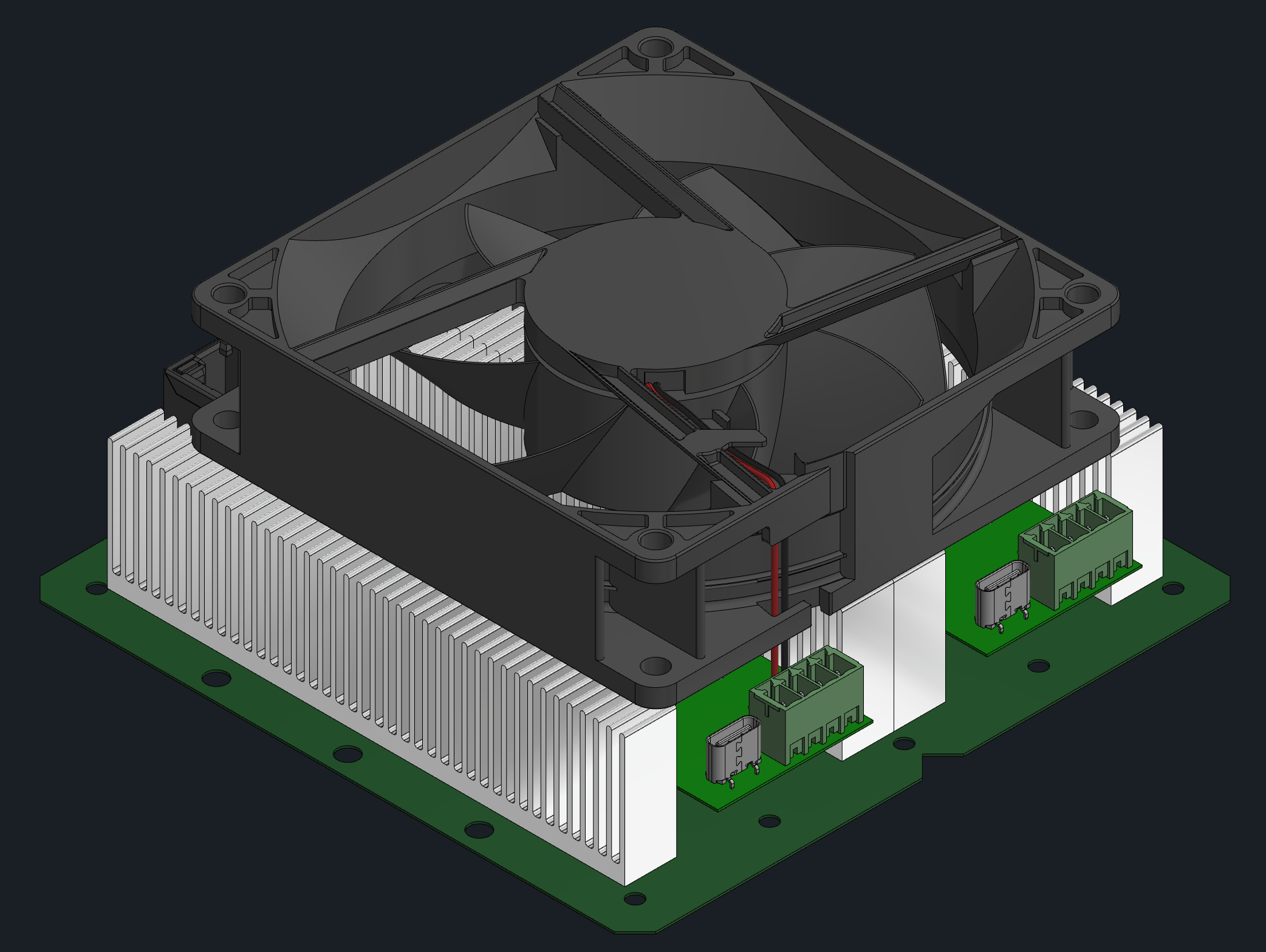
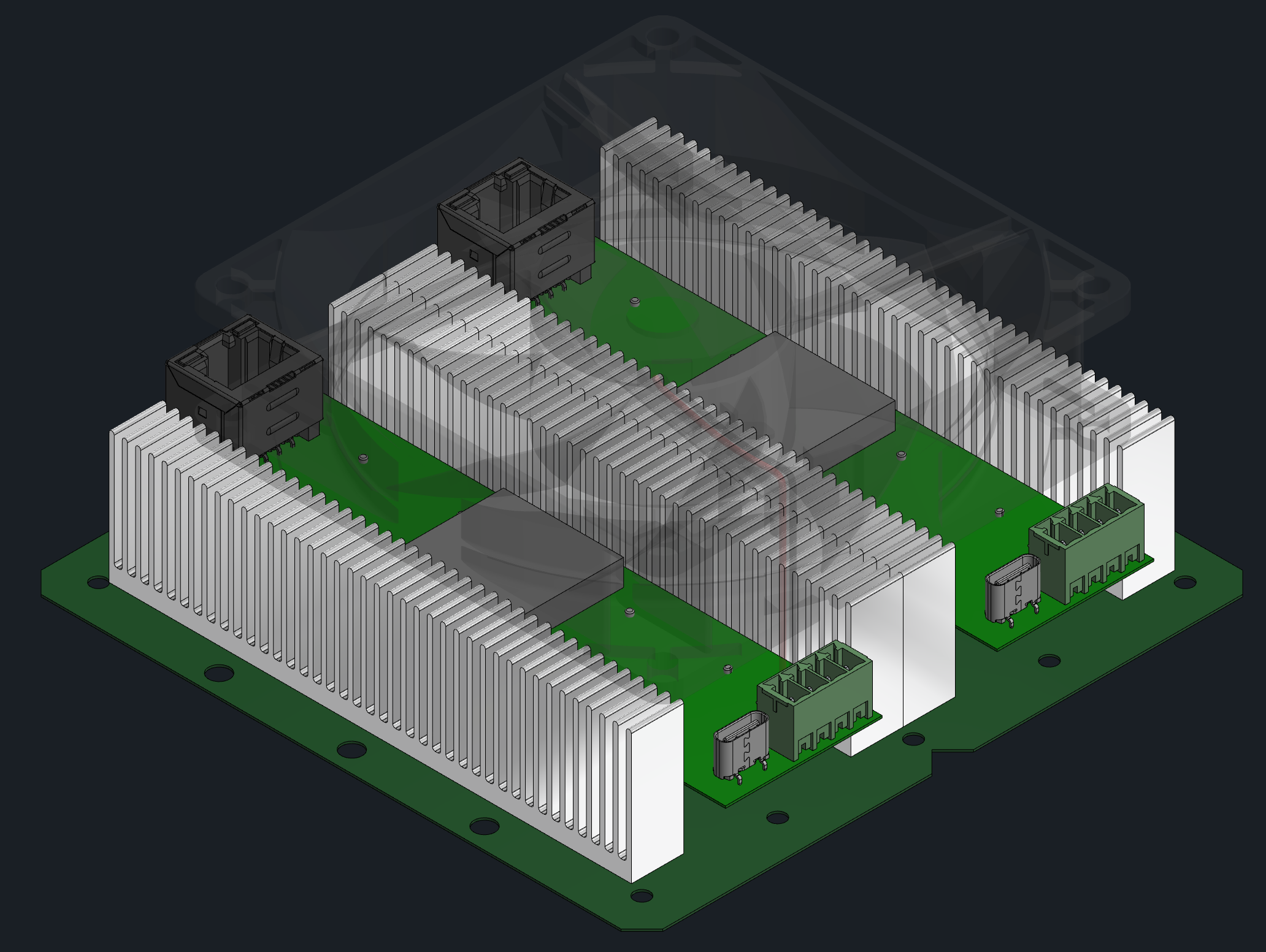
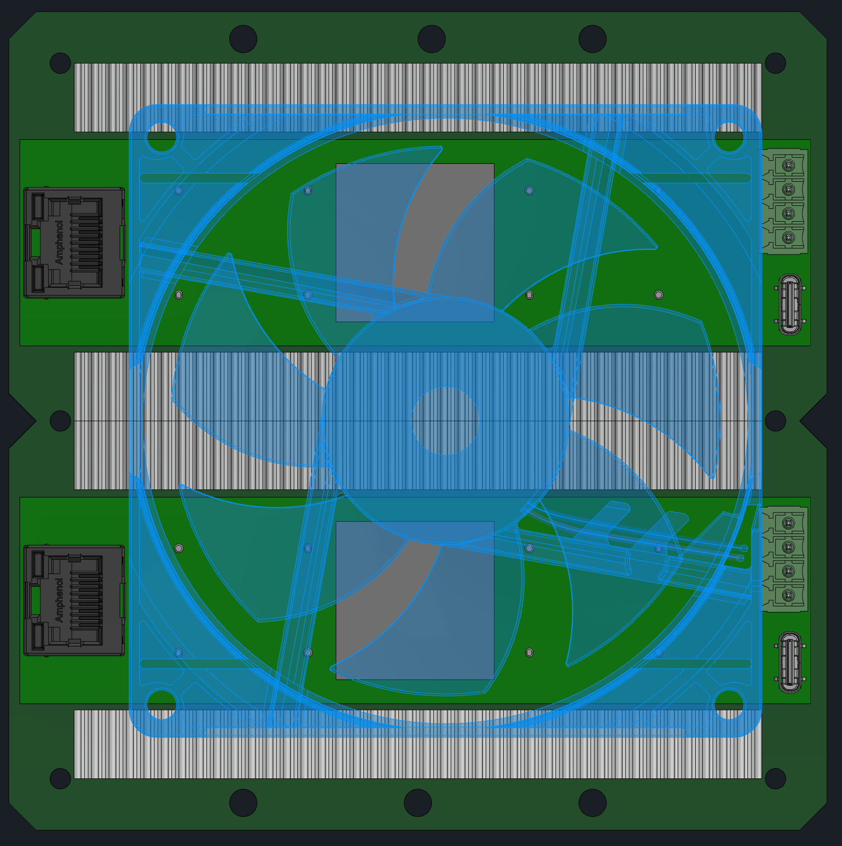
sure, vertical connector orientation makes tiling easier, to articulate the case. One of Daniel's pictures (with a blue fan superimposed with a sink) shows that there is no conflict with cabling either. Should we "freeze" this layout, and work out the remaining details based on it? I see Samtec connectors and FPGA itself are already placed symmetrically with respect to the ASICs in this picture as well. Heat sink should probably be a single piece, do we agree? There is no conflict with HV pins / cables. Then what is missing, from the mechanical / integration standpoint is: (1) screws which fix ASIC board on the sensor and a fiducial volume around the respective nuts, (2) pressfit fixtures to bolt two PCBs together, (3) whatever is needed to fix the sink assembly on top of everything else. Anything else?
As far as I understand, once we all agree on such a configuration in general, Daniel can work out a heat sink layout, decide on the Samtec connector height, and we think about sensor assembly mounting scheme as a whole on our end, while ASIC board and FPGA board design get decoupled from each other once the Samtec connector pins are assigned, and LV scheme is decided upon. Correct?
By the way, my gut feeling is that in the real detector setup all connectors will be oriented horizontally, since it is the space in the direction normal to the sensor plane which is at a premium. As long as the connectors themselves are within the sensor footprint, cables can always be disconnected to take a neighboring sensor out. My 2 cents.
Cheers,Alexander.
From: nagy g <hunagabo AT gmail.com>
Sent: Thursday, August 3, 2023 6:40 AM
To: Cacace, Daniel <dcacace AT bnl.gov>
Cc: Kiselev, Alexander <ayk AT bnl.gov>; czeller.miklos AT gmail.com <czeller.miklos AT gmail.com>; Damien Thienpont (IN2P3) <damien.thienpont AT in2p3.fr>; Pierrick Dinaucourt <pdinaucourt AT omega.in2p3.fr>
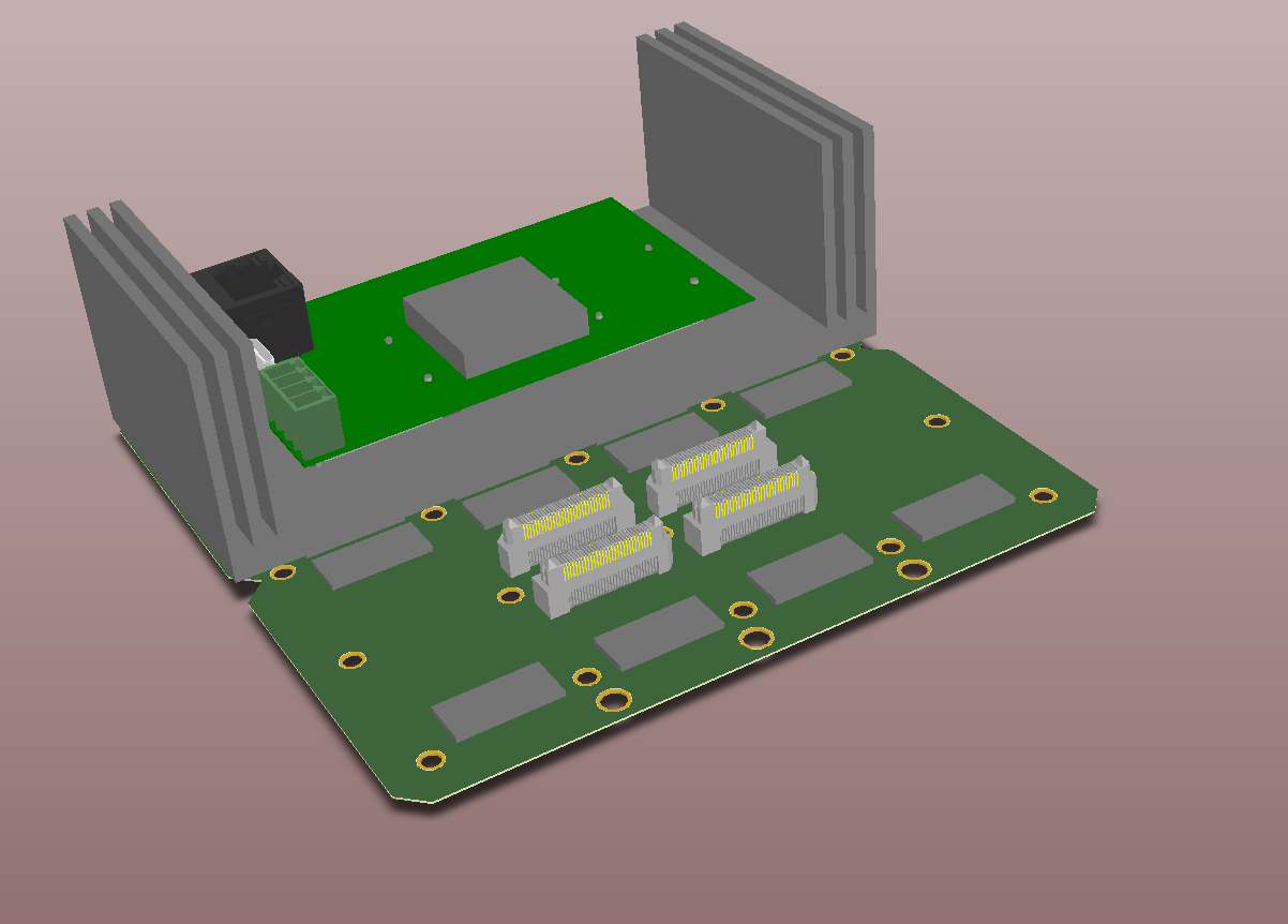
Subject: Re: pfRICH prototype HGCROC3 ASIC & FPGA cooling schemeHi Daniel and Alexander,The reason I proposed the straight connectors (vertical connection) was to allow the detector to put next to each other in all 4 direction. With the right-angle connectors (connecting from sides) it will be limited, but I do not know the application deep enough...So, if that is acceptable then we can go that direction. From the PCB point of view that is not a big deal :)
(just one comment, I would still prefer to use one big metal plate as a base of the heat-sink, instead of 3 separated one. Just to keep the module assembly simple.)
Br. gabor
Cacace, Daniel <dcacace AT bnl.gov> ezt írta (időpont: 2023. aug. 2., Sze, 20:02):
I realize this is missing the Samtec connector, but something more along these lines would be preferable.
From: Cacace, Daniel <dcacace AT bnl.gov>
Sent: Wednesday, August 2, 2023 1:56 PM
To: Kiselev, Alexander <ayk AT bnl.gov>; nagy g <hunagabo AT gmail.com>
Cc: czeller.miklos AT gmail.com <czeller.miklos AT gmail.com>; Damien Thienpont (IN2P3) <damien.thienpont AT in2p3.fr>; Pierrick Dinaucourt <pdinaucourt AT omega.in2p3.fr>
Subject: Re: pfRICH prototype HGCROC3 ASIC & FPGA cooling schemeHi Alexander and Gabor,
I agree, with the full heat sink and fan I was confident the cooling would be sufficient. Without having done any calculations, something like you show in your images I think would be marginal with a fan and probubly insufficient without a one.
I was thinking the same thing as Alexander, that a longer FPGA board would be better. Here are few images of what I would propose. Does it look reasonable? I show the heat sink in 3 sections, but it could be one part with a few cutouts, though I don't think it would really affect the cooling.
Thanks,
From: Kiselev, Alexander <ayk AT bnl.gov>
Sent: Wednesday, August 2, 2023 1:41 PM
To: nagy g <hunagabo AT gmail.com>
Cc: czeller.miklos AT gmail.com <czeller.miklos AT gmail.com>; Damien Thienpont (IN2P3) <damien.thienpont AT in2p3.fr>; Pierrick Dinaucourt <pdinaucourt AT omega.in2p3.fr>; Cacace, Daniel <dcacace AT bnl.gov>
Subject: Re: pfRICH prototype HGCROC3 ASIC & FPGA cooling schemeHi Gabor,
thank you, I can download the STEP file. Are you really suggesting to proceed without even a fan? Otherwise RJ45 cable sticking out vertically seem to become a problem. I'd still see it more natural to have a longer FPGA board, with all three cables routed away horizontally (like in your first iteration), and ERM5 connectors places symmetrically with respect to their respective ASICs (so neither the way the ones below the FPGA board are located nor the ones which are seen on the open half of the board). Also, one can still have a giant single heat sink with a fan even if it covers a pair of FPGA boards.
Daniel, will you have time to come up with a scheme which would take the best of the proposals made so far, from the cooling perspective?
Cheers,Alexander.
From: nagy g <hunagabo AT gmail.com>
Sent: Wednesday, August 2, 2023 10:58 AM
To: Kiselev, Alexander <ayk AT bnl.gov>
Cc: czeller.miklos AT gmail.com <czeller.miklos AT gmail.com>; Damien Thienpont (IN2P3) <damien.thienpont AT in2p3.fr>; Pierrick Dinaucourt <pdinaucourt AT omega.in2p3.fr>; Cacace, Daniel <dcacace AT bnl.gov>
Subject: Re: pfRICH prototype HGCROC3 ASIC & FPGA cooling schemejust two correction (from Miklos :)):- STEP model available here: https://web.tresorit.com/l/ZObME#B37XtULDHJE9ocNaJ999nw- And the connector on the board is a 60 pin version (ERM5-030-05.0-L-DV-TR)
Br, gabor
nagy g <hunagabo AT gmail.com> ezt írta (időpont: 2023. aug. 2., Sze, 15:47):
Hi Alexander,
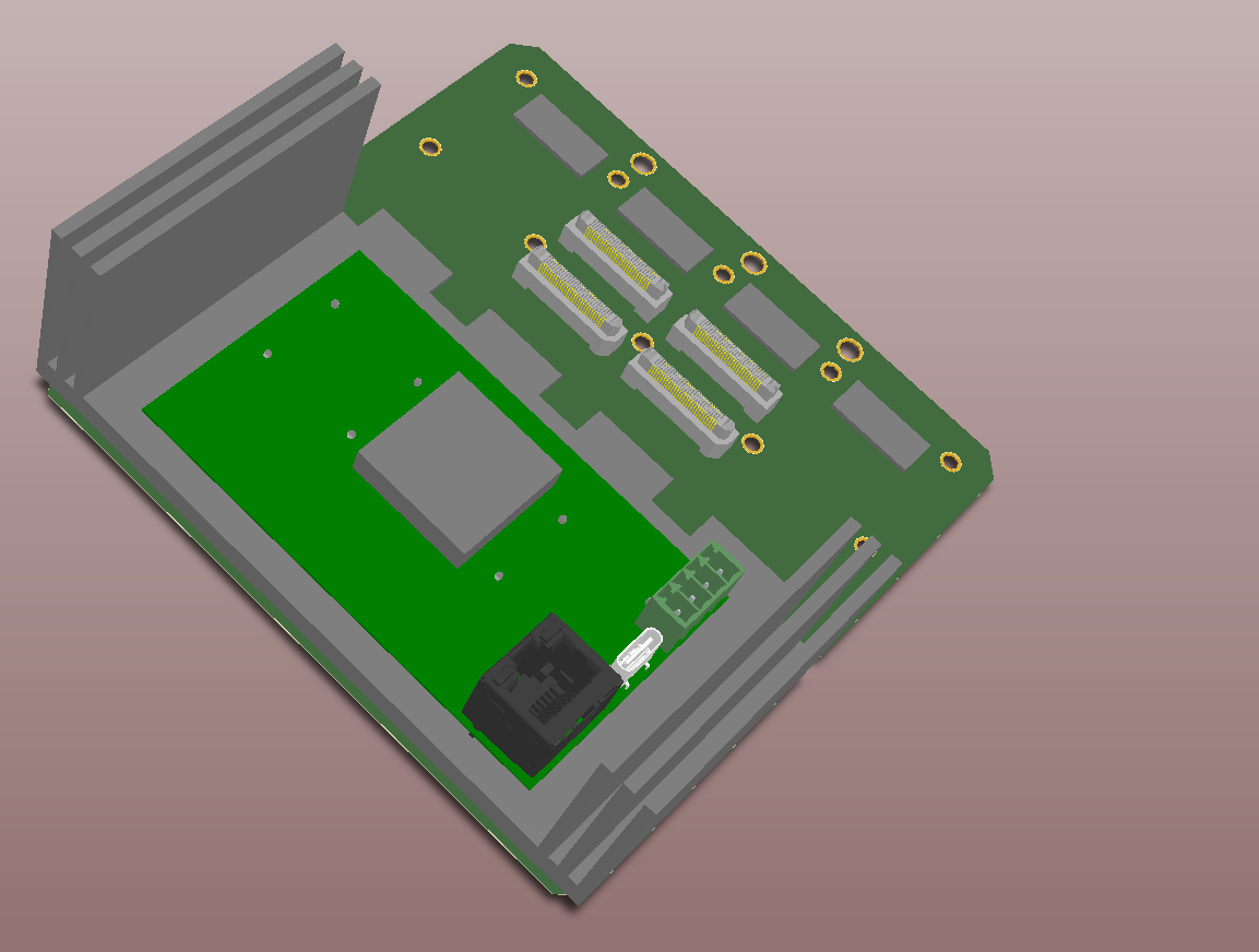
- The PEMs are not in the model jet (around the connectors), but the rest shows what we discussed last time.
- Heat sink plate (horizontal part of it) is covering the ASICs directly, and the size is the same as the PCB itself to enable putting the detectors next to each other.- The vertical part of the heat-sink needs additional work as well, but again, it is just a quick model to explain the possibilities.
- Regarding the connectors, the 40-pin version of SAMTEC's ERM5 series connector is used for the model to make sure the power can use multiple pins. (ERM5-020-05.0-L-DV-TR)
The STEP file is ~5MB so I would not attach it to the mail, but if you can send me any place to upload it, I can do that.(With one note for the model! As we have no model for the ASIC and the carrier board, all sizes are just approximately measured back from the slides you shared with us... so do not expect them to be correct.)
Best Regards, gabor
Kiselev, Alexander <ayk AT bnl.gov> ezt írta (időpont: 2023. júl. 31., H, 18:59):
Hello colleagues,
in the meantime, would it be possible to share a CAD model a la slide 9 here https://indico.bnl.gov/event/20090/contributions/78664/attachments/48726/82859/ayk-2023-07-20-erd110-meeting.pdf with Daniel (Cc), with a ~4cm wide FPGA board and ASICs swapped with the Samtec connectors, so that they are not shadowed by the FPGA boards? Daniel will then distribute an update of a cooling solution for the prototype.
Thank you,Alexander.
- [Eic-projdet-pfrich-electronics-l] Fw: pfRICH prototype HGCROC3 ASIC & FPGA cooling scheme, Kiselev, Alexander, 08/10/2023
Archive powered by MHonArc 2.6.24.
